Heterojunction (HJT) technology has been ignored for many years, but it has been developing in the past few years, showing its real potential. HJT addresses some common limitations of standard photovoltaic (PV) modules, such as reducing the recombination process and improving performance in hot climates.
If you want to know more about heterojunction technology, this article is for you. Here, you will learn about the design and operability of HJT solar cell, as well as the differences, advantages and applications compared with popular technologies.
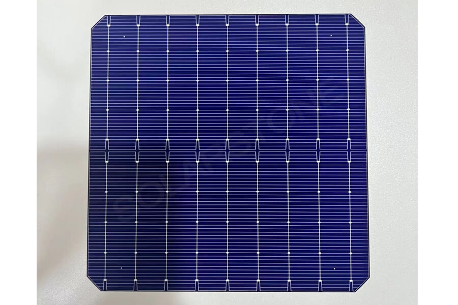
What is a heterojunction solar panel?
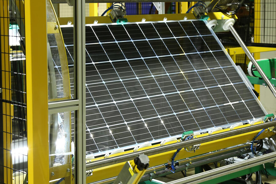
The assembly method of heterojunction solar panel is similar to the standard homogeneous junction module, but the unique feature of this technology lies in the solar cell itself. In order to understand this technology, we provide you with an in-depth analysis of the materials, structures, manufacturing and classification of heterojunction panels.
Materials required for manufacturing heterojunction solar cells
Heterojunction batteries use three important materials:
Crystalline silicon (c-Si)
Amorphous silicon (a-Si)
Indium tin oxide (ITO)
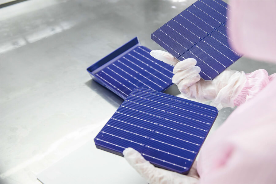
Crystalline silicon is often used to make standard homogeneous junction solar cells, as seen in traditional panels. There are two kinds of c-Si, polycrystalline silicon and monocrystalline silicon, but monocrystalline silicon is the only one considered for use in HJT solar cells, because it has higher purity, so it is more efficient.
Amorphous silicon used in thin film photovoltaic technology is the second important material for manufacturing heterojunction solar cells. Although a-Si itself has density defects, the hydrogenation process is used to solve these defects and generate hydrogenated amorphous silicon (a-Si: H), which is more easily doped and has wider band gap, and is more suitable for manufacturing HJT solar cells.
Indium tin oxide is the preferred material for transparent conductive oxide (TCO) layer of heterojunction solar cells, but researchers are studying the use of indium free materials to reduce the cost of this layer. ITO’s reflectivity and conductivity make it a better contact layer and outer layer of HJT solar cells.
Structure of heterojunction solar cells
The absorption layer of the heterojunction solar cell consists of a layer (blue layer) based on a c-Si chip, placed between two thin intrinsic (i) a-Si: H layers (yellow layer), and doped a-Si: H layers (red and green layers) placed on the top of each a-Si: H (i) layer. The number of TCO layers depends on whether the HJT solar cells is single-sided or double-sided, and the latter layer is a metal layer used as a single-sided heterostructure solar cells conductor.
Manufacture of Heterojunction Solar Cells
The manufacturing process of heterojunction solar cells involves several steps. These are:
Wafer processing
Wet chemical treatment
Core layer sedimentation
TCO Deposition
Metallization
Crystalline silicon processing involves cutting c-Si cells with diamond saws. Executing this process extremely finely will produce high-quality c-Si layers, which will translate into higher efficiency.
During the wet chemical treatment, organic and metal impurities are removed from c-Si wafers. Wet chemical treatment usually uses two methods, one is RCA method using concentrated sulfuric acid and hydrogen peroxide, and the other is cost-effective alternative method using ozone based process, which can obtain similar results.
After the wet chemical treatment, the amorphous silicon layer is deposited on both sides of the crystalline silicon base layer using the plasma enhanced chemical vapor deposition (PECVD) deposition process.
The second part of the deposition process uses physical vapor deposition (PVD) to apply ITO through sputtering to form a TCO layer of heterojunction solar cells. Another process uses reactive plasma deposition (RPD) to apply TCO layers, but this is an unpopular option.
The metallization process is different from the conventional manufacturing process because the hydrogen in a-Si: H limits the temperature to a maximum of 200-220 º C. Using specially treated low temperature silver paste, place the electrode on the battery through copper electroplating or screen printing process.
Classification of heterojunction solar cells
Heterojunction solar cells can be divided into two types according to doping: n-type or p-type.
The most popular doping uses n-type c-Si wafers. These are doped with phosphorus, which gives them extra electrons to make them negatively charged. These solar cells are not affected by boron oxygen, which will reduce the purity and efficiency of the cells.
P-type solar cells are more suitable for space applications because they are more resistant to the level of radiation perceived in space. The p-type c-Si chip is doped with boron, which provides one less electron for the battery and makes the battery positively charged.
How do heterojunction solar panels work?
The working principle of heterojunction solar panel under photovoltaic effect is similar to that of other photovoltaic modules. The main difference is that the technology uses three layers of absorption materials and combines thin film and traditional photovoltaic technology.
The process includes connecting the load to the terminal of the module, converting photons into electrical energy and generating current to flow through the load.
To generate electricity, photons strike the PN junction absorber and excite electrons, causing them to move to the conduction band and generate electron hole (eh) pairs.
The excited electrons are collected by the terminals connected to the P doped layer to generate a current flowing through the load.
After passing through the load, the electrons flow back to the back contact of the battery and recombine with the holes to end the specific eh pair. This happens as the modules generate power.
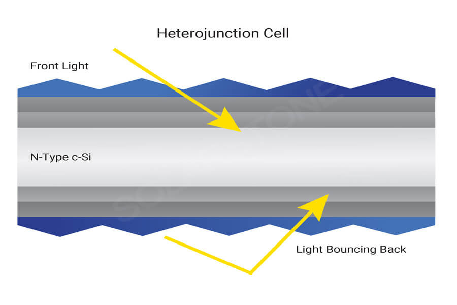
A phenomenon called surface recombination occurs in standard c-Si PV modules, which limits their efficiency. In this process, the stimulated electrons pair with holes on the surface of the material, causing them to recombine, while the electrons will not be collected and flow in the form of current.
To reduce surface recombination, HJT cells use a passive semiconductor film with a wider gap layer made of a-Si: H to separate highly composite active (ohmic) contacts from wafer based layers. The buffer layer makes the charge trickle slow enough to generate a high voltage, but fast enough to avoid recombination before collecting electrons, thereby improving the efficiency of the HJT cell.
In the process of light absorption, all three semiconductor layers will absorb photons and convert them into electrical energy.
The first photon arriving will be absorbed by the external a-Si: H layer and converted into electrical energy. However, most photons are converted by the c-Si layer, which has the highest solar energy conversion efficiency in the battery materials.
The remaining photons are finally converted by the a-Si: H layer on the back of the module. This three-step process is the reason why single-sided heterojunction solar cells can achieve a solar efficiency of 26.7%.